
Anchoring NY’s $10B Plan: Inside NanoFab Reflection’s 22-Foot Cleanroom
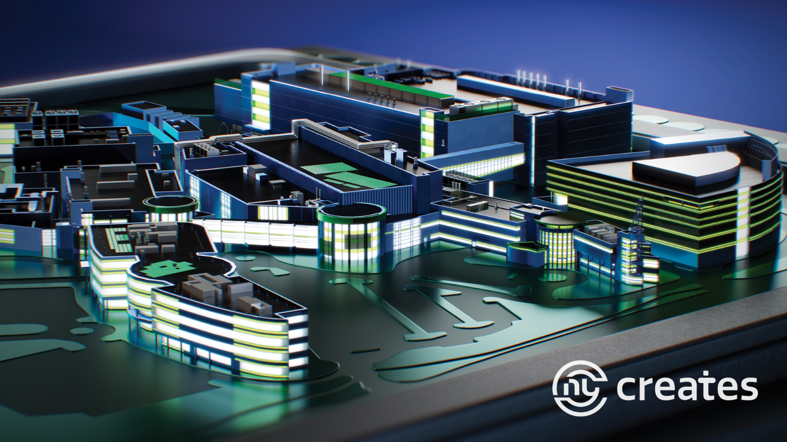
NanoFab Reflection, a 310,000-sf semiconductor research facility under construction at the Albany NanoTech Complex, will house North America’s first High NA EUV lithography system at a nonprofit-owned R&D center, supporting next-generation chip development by academic and industry researchers worldwide. Image: Courtesy of NY Creates
Over the past two years, commuters driving through Albany, New York, have witnessed a massive new structure rising within the Albany NanoTech Complex. This four-story, 310,000-sf shimmering behemoth of glass and white panels is known as NanoFab Reflection. Expected to cost $614 million to construct, the facility represents the cornerstone of a broader $10 billion computer chip research center plan first announced by Governor Kathy Hochul in late 2023.
Developed by NY Creates—a state-supported nonprofit that owns and operates Albany NanoTech—and built through a joint venture between Gilbane Building Co. and DPS Advanced Technology Group (DPS/Gilbane), NanoFab Reflection is slated to become a critical asset to the global computer chip industry. Unlike traditional commercial fabrication facilities built for private corporate use, NanoFab Reflection will feature North America’s first and only High Numerical Aperture Extreme Ultraviolet (High NA EUV) lithography machine located at a nonprofit-owned research and development center. Once operational, academic and industry scientists from around the world will line up for coveted tool time to engineer the next generation of advanced microprocessors.
Scaling up: the massive demands of high NA EUV lithography
At the heart of NanoFab Reflection is its 50,000-sf cleanroom. Walking into the space reveals an environment where everything is built on a vastly grander scale than the industry norm. Most notably, the cleanroom features 22-foot ceilings, which are significantly higher than the standard 15-foot industry benchmark.
“The decision to implement 22-foot ceilings in the NanoFab Reflection cleanroom was directly informed by the dimensional and operational requirements of the High NA EUV tool, as well as the need to accommodate an overhead crane for installation and maintenance,” says Andre Savoe, vice president and business director for US semiconductor at Arcadis. “To optimize flexibility and minimize complexity, the design team elected to maintain a consistent ceiling height throughout the space, rather than varying heights. This approach ensured seamless integration of the tool and associated equipment, while also streamlining construction and future adaptability.”
The extreme dimensions of the facility are necessitated by the tool it was custom-built to house: the TwinScan EXE: 5200B, manufactured by the Dutch company ASML. Valued between $380 million and $400 million, this revolutionary machine functions as an atomic-scale printer. It shoots extreme ultraviolet lasers at a rapid stream of molten tin droplets falling at 50,000 drops per second, creating a plasma-based light source—often described as a supernova lightbulb held in a box—to etch features onto 12-inch silicon wafers.
While previous EUV scanners were roughly the size of a standard transit bus, the new High NA EUV model is the size of a double-decker bus and weighs a massive 200 tons—the equivalent of two Airbus A320 airplanes. To achieve a higher numerical aperture for sharper resolution designs at 8 nanometers and below, its internal optical systems required a complete overhaul. The specialized mirrors manufactured by Germany’s ZEISS are twice as large and ten times heavier than those in older EUV systems. The integrated projection system alone contains 40,000 parts and weighs 12 tons.
To safely transport and assemble this colossal system, the tool must be shipped from Europe via five cargo planes, split across 250 crates in 43 containers, and delivered to the facility using 20 semi-trucks. The cleanroom infrastructure had to be engineered from day one to handle this logistical undertaking.
The facility integrated specialized entryways to preserve cleanroom integrity during this phase.
“To support the on-site assembly of the High NA EUV tool, we designed a dedicated clean tool wipe-down area, allowing tool crates and components to be unpackaged and thoroughly cleaned before entering the cleanroom environment,” says Christian Calabrese, project director at Gilbane Building. “This infrastructure, combined with overhead cranes and generous clearances, was integral to meeting the stringent cleanliness and operational requirements throughout the assembly process.”
Overcoming engineering and environmental challenges
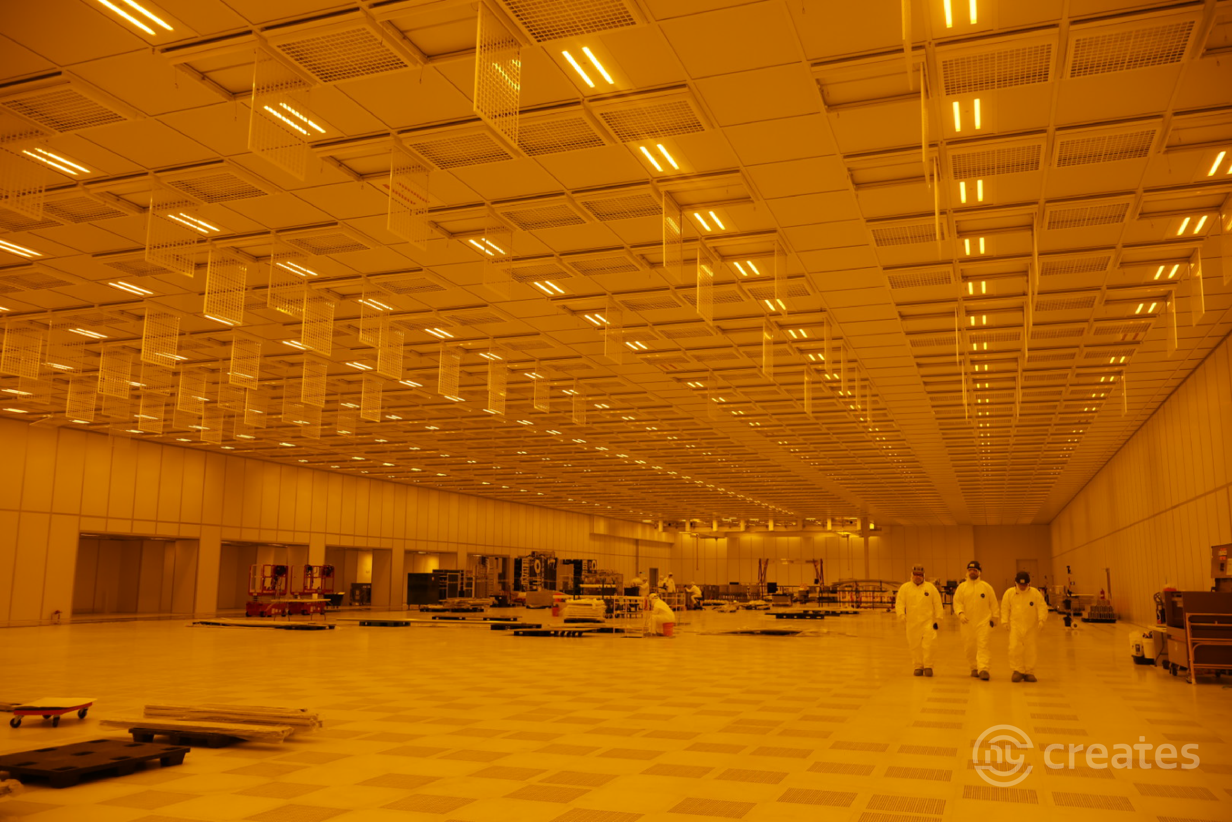
To support the facility’s High NA EUV lithography system, the cleanroom is designed to maintain ultra-low particle levels through more than 90 air changes per hour, specialized filtration systems, and carefully engineered airflow distribution across its 22-foot-high ceiling. Image: Courtesy of NY Creates
Operating a High NA EUV tool requires absolute environmental stability. Even the smallest microscopic particle can ruin a chip or severely damage the multi-million-dollar optics. While a human hair spans 70 to 100 microns in width, ASML’s tool demands an environment with 10 or fewer particles smaller than a tenth of a micron per cubic meter, with the most sensitive zones requiring a “zero” particle environment.
To meet these criteria, the cleanroom acts as a living, breathing mechanism where air is completely changed over 90 times an hour. Dozens of ultra-low penetration air filters line the ceiling panels to constantly polish the air, keeping the space at a strict 68 degrees Fahrenheit and 45 percent humidity.
However, moving that volume of air uniformly becomes incredibly complex when the ceiling is raised to 22 feet.
“Designing the HVAC and filtration systems to meet the stringent particle and air exchange requirements for semiconductor manufacturing presented several unique challenges, particularly given the increased ceiling height,” says Stephen Mayer, mechanical engineering department leader at DPS Group. “To address this, we leveraged best practices from other advanced facilities both domestically and internationally. Collaboration with the filter fan unit (FFU) manufacturer was essential, enabling us to develop specialized diffuser solutions that promote uniform airflow distribution from the elevated ceiling to the cleanroom floor, thereby maintaining ultra-low particle levels.”
Advanced vibration isolation
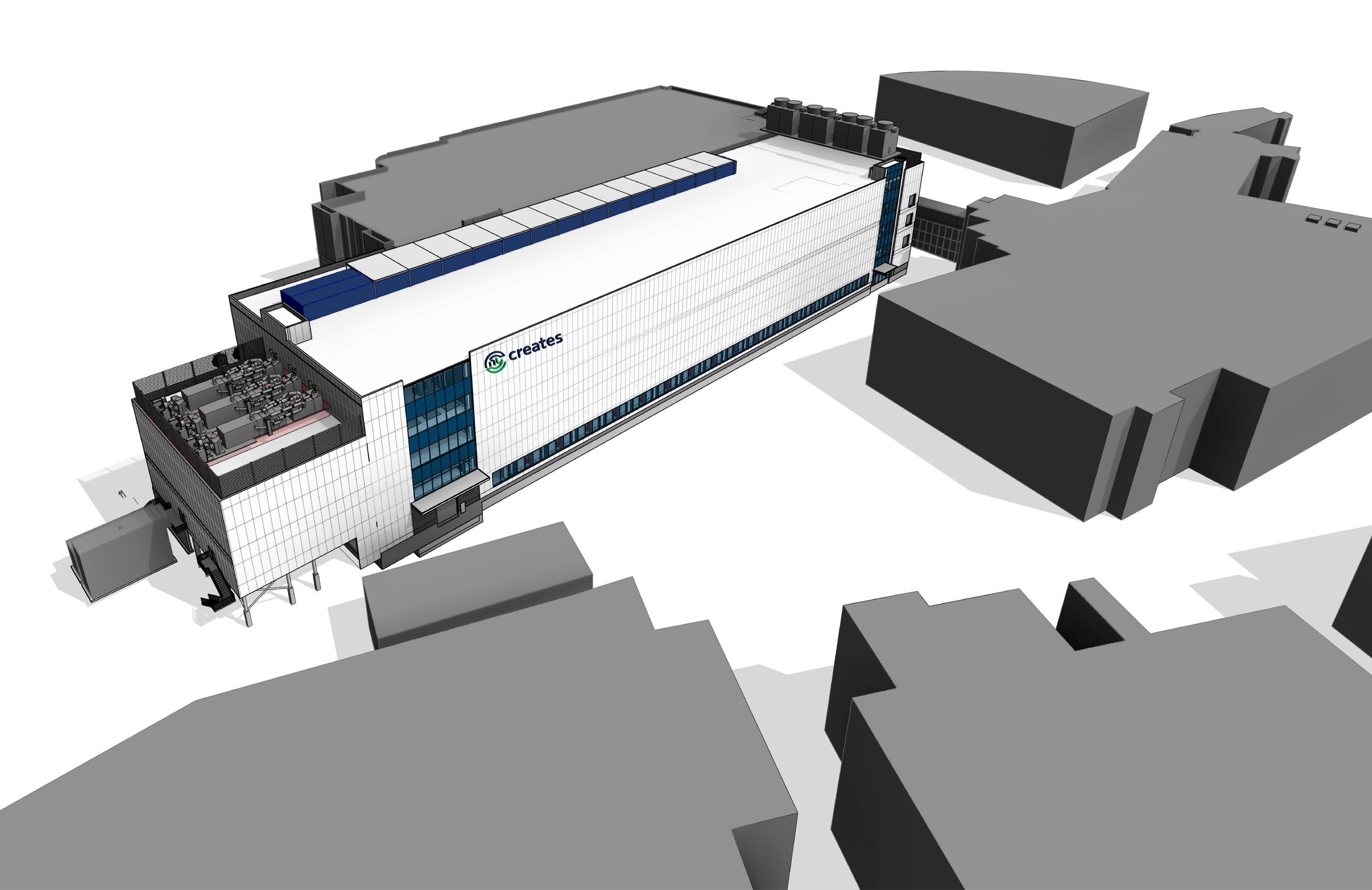
To protect the High NA EUV lithography process from vibration and contamination, the project team incorporated structural isolation strategies, vibration-dampening systems, and carefully designed airlock connections between NanoFab Reflection and the adjacent NanoFab Xtension facility. Image: Courtesy of NY Creates
Equally challenging was shielding the atomic-scale lithography process from structural vibrations. The project team consulted with specialized vibration engineers to develop a structural strategy that isolated different segments of the complex.
“Our team, in consultation with a specialized vibration engineer, implemented a multi-building strategy, effectively segmenting the facility into three distinct structural entities,” Mayer says. “This approach minimized the transmission of vibration between functional areas.”
Furthermore, heavy mechanical equipment was structurally isolated using high-performance dampening components.
“Additionally, comprehensive vibration isolation measures, including the use of springs beneath first-floor chillers with composite supply and return connections, were applied to all major equipment, ensuring a stable environment for precision manufacturing,” says Mayer. The structural team also had to customize unique precast concrete elements within the High-NA Area to ensure the building could simultaneously support the immense physical loads and meet the rigid vibration criteria.
Further complicating the environmental design was the physical connection between NanoFab Reflection and the existing, adjacent NanoFab Xtension building, which operates an older ASML EUV scanner. The team linked the two structures without destabilizing either environment.
“Ensuring environmental compatibility between the NanoFab Reflection and the existing NanoFab Xtension was a primary design consideration,” says Tara Travis, design project manager at Arcadis. “We prioritized maintaining distinct airflow and pressurization regimes while facilitating personnel movement between the facilities. This was accomplished through the strategic placement of double-door airlock rooms at key transition points, while the remainder of the shared cleanroom wall was fully isolated to prevent cross-contamination and preserve operational integrity.”
Cross-disciplinary collaboration and future lessons
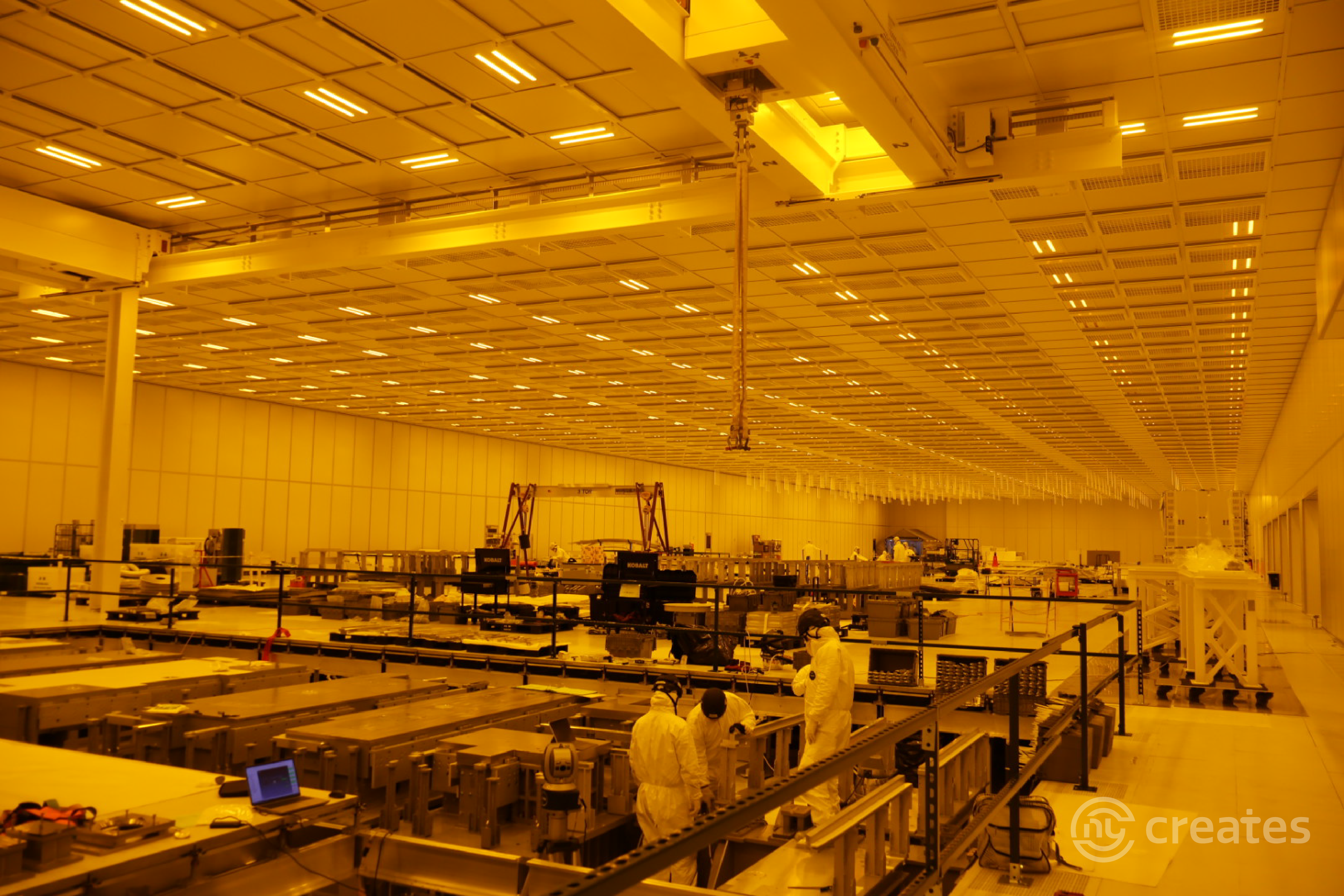
Frequent coordination among designers, engineers, contractors, facility operators, and equipment vendors helped the NanoFab Reflection team integrate complex building systems, overcome construction challenges, and prepare the semiconductor research facility for final certification and occupancy. Image: Courtesy of NY Creates
The successful execution of NanoFab Reflection relied on continuous feedback loops between the construction teams, management, tool vendors, and the facility engineers representing the scientific community. Communication was built into the weekly cadence of the project.
“Collaboration was central to the success of the NanoFab Reflection project. Throughout the design phase, weekly coordination meetings brought together design engineers, NY Creates facility engineers, management, and construction managers,” says Calabrese. “This multidisciplinary approach ensured project alignment, constructability, and that the final spaces would meet the operational needs of the end users. In addition, similar coordination was undertaken across architectural, process/chemical, electrical, and control disciplines, ensuring comprehensive integration of all facility systems and requirements.”
This high level of alignment spanned across architectural, process/chemical, electrical, and control disciplines, ensuring comprehensive integration of all facility systems. This collaboration proved vital when confronting unexpected construction hurdles, such as fitting the massive facility within the existing site footprint, integrating brand-new central utilities (boilers and chillers) directly adjacent to the cleanroom, and deploying sustainable stormwater reuse tanks to support cooling tower operations while minimizing regional rainwater discharge. The team also successfully navigated the complexities of pursuing LEED certification alongside managing the engineering challenges of an extra-tall cleanroom ceiling.
Reflecting on the massive project, Calabrese notes that early stakeholder engagement is the primary takeaway for the future of semiconductor facility design:
“One of the most valuable lessons was the importance of early and comprehensive coordination across all engineering disciplines during initial space planning and layout. The collaborative partnership between NY Creates, the contractor, and the design team will be instrumental to the project's success,” he says. “For future facilities supporting next-generation semiconductor research tools, we recommend an even greater emphasis on early stakeholder engagement and iterative design reviews to anticipate evolving requirements.”
With the cleanroom spaces currently nearing completion and final certification, the keys to NanoFab Reflection are on schedule to be handed over to NY Creates. Component deliveries are underway, paving the way for the multi-month on-site tool assembly and the highly anticipated “first light” of North America's most advanced chip research facility.